Location: Science Hall, Room 108,
502 Yates St., Arlington, TX 76019
Mailing address: P.O. Box 19059
Phone: 817-272-2266
Fax: 817-272-3637
Email: physics@uta.edu
WELCOME TO UTA PHYSICS
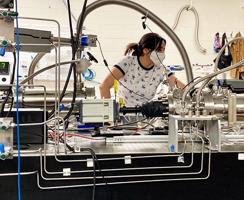
The UTA Department of Physics will prepare you for a rewarding career with our innovative education and world-class research programs. These programs are led by highly esteemed faculty and conducted in top-notch facilities which equip students for careers in industry, research, or academia. We have many specialized undergraduate degree programs that offer an excellent foundation in physics, and our graduate programs provide advanced training in a collaborative research environment which has the Carnegie Classification's highest rating: R1 Doctoral Universities – Very high research activity. Research and education go hand-in-hand and all students are encouraged to become active in research early in their academic careers.
Undergraduate Degree Programs
Majors
Bachelor of Science in PhysicsBachelor of Science in Physics with Medical School Preparation
Bachelor of Science in Physics with Engineering Emphasis
Bachelor of Science in Physics with Physical Science Teacher Certification/UTeach
Bachelor of Science in Physics with Physics/Mathematics Teacher Certification/UTeach
Bachelor of Arts in Physics
Bachelor of Science in Physics with a Master of Science in Materials Science and Engineering (Fast Track Program)
Graduate Degree Programs
Research Areas
• Astrophysics • Chaos and Nonlinear Physics • Condensed Matter Physics • High Energy and Nuclear Physics • Medical Biophysics • Nanostructured Magnetic Materials • Space Physics • Theoretical Condensed Matter Physics
News
Helpful Student Links
ADMINISTRATION
Dr. Alex Weiss
Distinguished Professor and Chair
817-272-2266
weiss@uta.edu
Dr. Jonathan Asaadi
Associate Professor and Associate Chair
817-272-2266
jonathan.asaadi@uta.edu
Dr. Nilakshi Veerabathina
Professor of Instruction and Associate Chair
817-272-1837
nilakshi@uta.edu
Shawnta Coleman
Office Administrator
817-272-9014
shawnta.coleman@uta.edu