Step 1
Watch video 1) PCB Basics and video 2) Fusion student install to get the student version of Fusion. You will need to create an account, but the account gives you access to AutoDesk TinkerCad also.
Download Fusion
Making PCB's may be one of the most valuable skills you can have. This page is dedicated to helping you bring you ideas into reality. After these three steps you will be able to create your own custom schematics, design a PCB from your schematics and send your files to a PCB manufacturer or mill them on one of the electrical engineering's milling machines.
Watch video 1) PCB Basics and video 2) Fusion student install to get the student version of Fusion. You will need to create an account, but the account gives you access to AutoDesk TinkerCad also.
Watch Videos 3) Schematics and 4) PCB to learn to make a 555 timer circuit on a 1 sided PCB. You even learn to use a USB-C connector.
Watch video 5) Autodesk Fusion Gerber Files / PCB Manufacturing to learn how to send your design to a professional PCB manufacturer.
Design students should send the UTA EE Lab their top and bottom copper layer, profile and drills files in a zip folder to the parts request system to have their PCB milled here at UTA.
This video covers what PCB's are made out of and common PCB terms
This video show you how to download, install and activate the student version of Fusion
This video cover libraries and how to make a schematic.
In this video you will follow along to design a PCB Layout.
In this video you will learn how to export the files into industry standard Gerber files which you can send to a PCB manufacturing web site
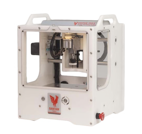
Once your done with your PCB layout in Fusion, we can mill your PCB with the Bantam Tools milling machine in the EE maker space.
Dr. Wei-Jen Lee
Professor and Chair
817-272-3934
wlee@uta.edu
Dr. David Wetz
Professor & Associate Chair
817-272-1058
wetz@uta.edu
Dr. Yuze (Alice) Sun
Professor & Associate Chair
817-272-1317
sun@uta.edu